

The mythical Ibanez Tube Screamer is not free of issues ! Let's talk about why I dislike its sound so much.
shopping_cart
0
Latest posts
-
 Why does the Tube Screamer sound bad ?Read more
 -
 Master fuzz clean-up like a pro !Read more
Let's talk about volume clean-up, vintage fuzzes and buffer pedals, and how everything interacts together.
-
 Circuit Analysis : Electro Harmonix LPB1Read more
Let's dive deep into electronics and explore the Electro Harmonix LPB1 and Screaming bird at once !
-
 Master the art of reampingRead more
Let's talk about how to use a DI box and a reamp box and what they are doing under the hood.
-
 How to record an electric guitar : all about microphonesRead more
All you ever wanted to know about recording your electric guitar amplifier with microphones, but were afraid to ask !
-
 Guitar preamps: are they a scam?Read more
Understand what really is a guitar preamp pedal, its difference with a studio preamp and an overdrive pedal, and how...
-
 The art of stacking effects pedalsRead more
Discover how to master pedal stacking with overdrives, saturations, compressors, and time-based effects. Learn the...
-
 The ultimate power supply guideRead more
Let's explore what make a good power supply, how to choose one and how to read their labels to prevent frying up your...
-
 Flanger is the BEST modulation pedalRead more
Hot take : flanger is definitely the best modulation effect ever invented. I can have it replace a phaser, a chorus...
-
 The ultimate guide about modulation effectsRead more
Modulation effect pedals form a distinct category of guitar pedals. What are the differences between a chorus, a...
Blog categories
Search in blog
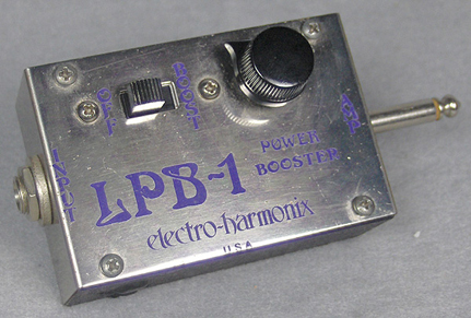
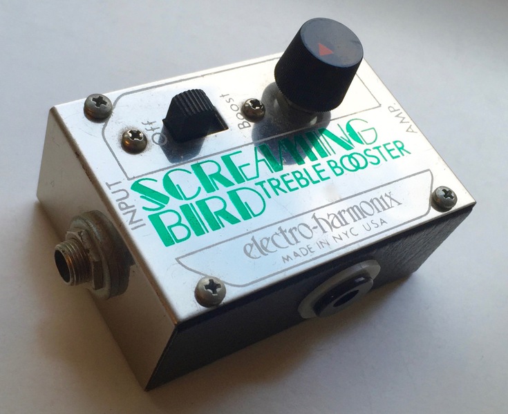
Circuit Analysis : Electro Harmonix LPB1
Welcome to the workshop. Today I am offering content that is a bit different from what I usually do: a complete A-to-Z analysis of an electronic circuit. For this, I will discuss the simplest boost circuit to analyze, the Electro-Harmonix Linear Power Booster 1, and its little brother, the Screaming Bird treble booster.
The content of this blog post is deliberately more technical than the associated YouTube video, where I explain the same concepts without calculations and in a more accessible way. If you find this article too technical, that is normal. It is intended for those who want to go deeper.
1. Brief history
In 1968, the young Mike Matthews set out to design a new type of effect pedal, a sustainer that would not distort the instrument’s sound as much. At the time, the few available effects were limited to the DeArmond Tremolo, large studio machines, and a few fuzz pedals that sounded too shrill, too thick, too velcro-like—nothing subtle.
Mike asked his friend Bob Myers, an electronics engineer at Bell Labs, to design the circuit that would later become the Big Muff Pi. During his experiments, Mike noticed that Bob was using a small box to preamplify the guitar signal because it was too weak for the rest of the prototype circuit. Mike loved the sound of this preamplifier so much that he immediately housed it in a small metal enclosure to plug directly into his electric guitar: the Linear Power Boost, or LPB-1, was born.
Later, the schematic was integrated into the Big Muff Pi and adapted into many variations to emphasize treble with the Screaming Bird treble booster, bass with the Bass Mole, and was adopted by other brands to create numerous boosters using silicon and germanium bipolar transistors, FET transistors, and more. Today, the LPB-1 remains a reference and is certainly one of the best circuits to build when starting out in DIY.
2. Schematics
The schematic is disarmingly simple: barely eight components, including the single volume potentiometer!
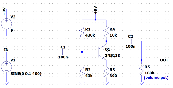
Capacitors C1 and C2 are coupling capacitors. Their main role is to prevent external DC voltages from disturbing the circuit, and vice versa. Capacitors only allow AC voltages and currents to pass, which is convenient since our guitar signal oscillates around ground (0V) and our battery (V2 in the schematic) cannot provide less than 0V or more than 9V. C1 and C2 also attenuate low frequencies, depending on their values.
The resistors are labeled R1 to R4 and have values in ohms (43k = 43 kohm = 43,000 ohms). R4 sets the theoretical maximum gain of the circuit, while R1 and R2 determine the transistor Q1 bias point. Bias refers to the voltages and currents flowing through the transistor when the battery is connected and no input signal is present. These are the DC conditions of the circuit. R3 has a more specific role: it provides local negative feedback. In simpler terms, it sacrifices part of the circuit’s gain to make it more stable, with less noise, distortion, and sensitivity to exact component values and transistor choice. This explains why almost any silicon transistor can work here: 2N5133 as in the original, 2N5088 in modern versions, 2N2222 for low noise, or 2N2904 as an inexpensive general-purpose transistor.
Finally, the amplified signal is more or less attenuated by the volume control until it is fully cut or fully passed through. The LPB-1 therefore works by amplifying first and attenuating afterward, not the other way around. It is not a variable-gain stage: the gain is always at maximum, and the potentiometer acts only as a passive attenuator.
3. Bias point analysis
To understand how the component values were chosen, we can analyze the transistor’s bias point. Circuit design often starts from a set of specifications defining the required function. For the LPB-1, we might imagine a required voltage gain of 25 and a frequency response wide enough to amplify all electric guitar frequencies equally, from 20 Hz to 20 kHz.
First, R4 can be chosen somewhat arbitrarily. A common value is 10k, as used here, but another value could be chosen as long as the transistor is not underpowered and sufficient current can flow. Too large a value, such as 100k or more, would prevent proper amplification, while too small a value would demand more current than the transistor can handle and risk damage.
. The circuit gain is approximately equal to –R4/R3. The negative sign indicates phase inversion: the output becomes positive when the input is negative, and vice versa. This gives R3 = R4/25 = 400 ohms. Since that is not a standard value, 390 ohms is chosen.
In reality, the gain also depends on the transistor’s current gain, denoted β or hFE. However, the relationship between transistor gain and circuit gain is not straightforward, and as long as transistor gain is sufficiently high (above about 50, which is almost always the case today), the simplified formula is valid. The full formula is:
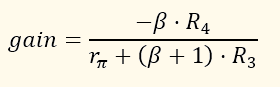
where Rpi = VT/IB, IB is the DC base current, and VT is the thermal voltage given by the following formula where T is the temperature in K, e the electrical charge and k is Boltzmann's constant:
![]()
Using both formulas at 22°C with a low-gain transistor (β = 50), the simplified formula predicts a gain of 25.6 and the full formula 23.3, which is close. With higher β, the difference becomes smaller. The transistor gain mainly indicates how effectively it operates.
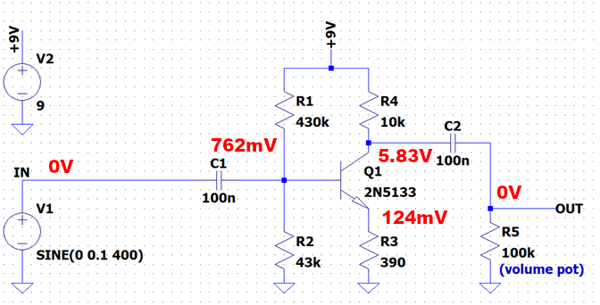
To calculate R1 and R2, we estimate the desired DC collector voltage. With a 9V battery, the collector voltage cannot exceed 9V or go below 0V. To maximize signal swing without saturation, it makes sense to bias at mid-supply, 4.5V. Using Ohm’s law, the current through R4 and the collector is Ic = 0.45 mA. This current is nearly equal to the emitter current, producing 176 mV across R3.
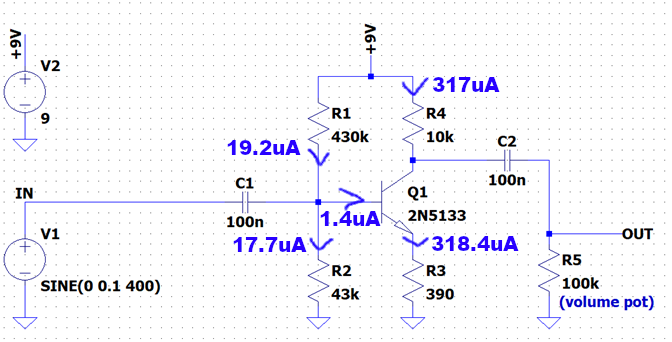
A properly biased transistor has about 650 mV between base and emitter, depending on temperature and device specifics, as described by the Shockley equation. Adding emitter voltage and base-emitter voltage gives a base voltage of about 826 mV. R1 and R2 are then chosen so their voltage divider provides this base voltage. The transistor gain affects this calculation because a small base current flows, which may require simulation with software such as LTSpice. My calculation gives R1 = 230k for R2 = 43k. In the original schematic, R1 = 430k, resulting in less conduction and a collector voltage around 5.8V. With strong input signals, the transistor will saturate sooner in the original circuit than in my calculated version. Here are the voltage (red) and current (blue) operating point.
4. Input and output impedances
The input impedance is calculated by considering R1 and R2 in parallel with the transistor’s reflection of R3 at the base, equal to the sum of Rpi and (β+1)·R3. This gives an input impedance of about 29k, which is very low. Electric guitars typically require at least 500k input impedance !
Output impedance is the parallel combination of R4 and an equivalent resistance determined by rπ, R3, Early resistance, and transconductance. It is roughly equal to R4, about 10k. The volume potentiometer further varies this from 10k to 55k down to 0 ohms. This is also relatively high and ideally, output impedance would stay below 1k.
5. Frequency response
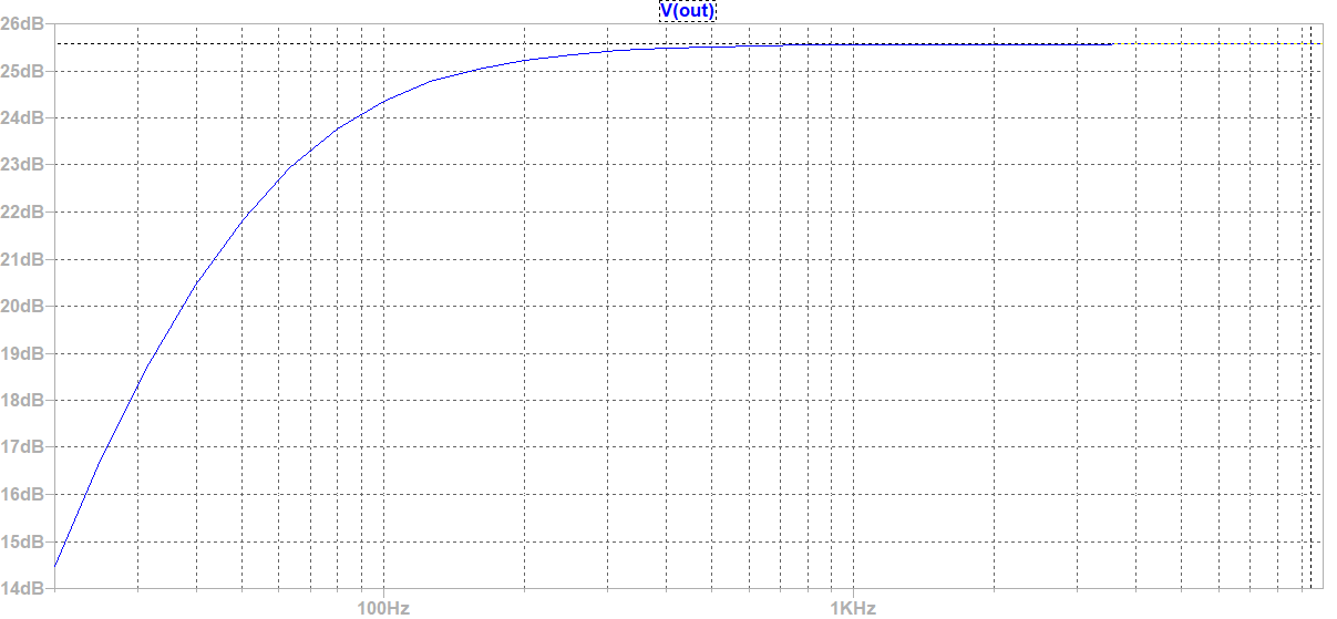
Knowing the input impedance helps determine the low-frequency cutoff. C1 and the input impedance form a high-pass filter cutting lows below 55 Hz, low enough for guitar. C2 and the potentiometer form another high-pass at 16 Hz, inaudible. No low-pass filter limits high frequencies, so gain remains high up to 20 kHz, with the transistor itself eventually limiting gain above the audible range.
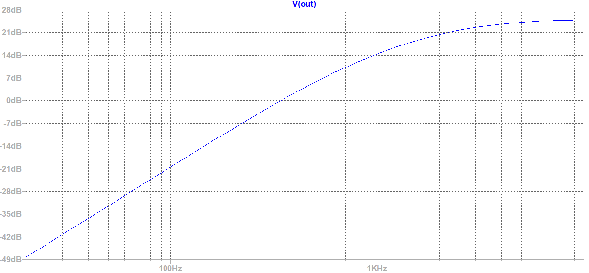
Changing C1 and C2 to 2 nF gives the Screaming Bird circuit. C1 then cuts below 2750 Hz and C2 below 800 Hz, clearly altering the frequency response.
If you build your first pedal and modify it yourself, you can experiment with C1 and C2 values, even using a switch, to create a treble booster with varying brightness. This analysis illustrates how static bias analysis and dynamic analysis of gain, impedance, and frequency response apply broadly in electronics engineering. I chose a relatively simple case to introduce the first concepts and notations. Feel free to leave me a comment if you have any question and I'll gladly reply !
Posted in:
Audio electronics
Related posts
-
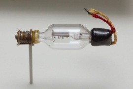 The vacuum tube explained
No need to known electronics ! Let's have a look at how a vacuum tube operates, and learn the differences between...Read more
The vacuum tube explained
No need to known electronics ! Let's have a look at how a vacuum tube operates, and learn the differences between...Read more -
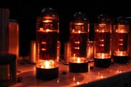 Audio vacuum tubes for dummies
What are the most used vacuum tubes in audio and guitar amplifiers ? What does 12AX7, GZ34 or EL84 do to the sound ?...Read more
Audio vacuum tubes for dummies
What are the most used vacuum tubes in audio and guitar amplifiers ? What does 12AX7, GZ34 or EL84 do to the sound ?...Read more -
 True Bypass vs Buffer Bypass : understanding your guitar pedal's signal path
Learn the difference between true bypass and buffer bypass to optimize your guitar signal. Avoid tone loss and...Read more
True Bypass vs Buffer Bypass : understanding your guitar pedal's signal path
Learn the difference between true bypass and buffer bypass to optimize your guitar signal. Avoid tone loss and...Read more -
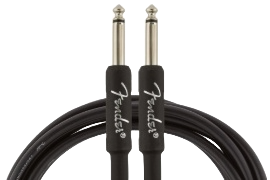 Choosing guitar cables: enhance your sound quality
Learn how guitar cables influence your tone. From capacitance to shielding and tips to maintain signal clarity,...Read more
Choosing guitar cables: enhance your sound quality
Learn how guitar cables influence your tone. From capacitance to shielding and tips to maintain signal clarity,...Read more -
The ultimate power supply guide
Let's explore what make a good power supply, how to choose one and how to read their labels to prevent frying up your...Read more
Leave a comment
Comments
trnsistor LPB-1
By: James Baker On 05/12/2026Hi, in general, how similar are the transistors 2N5133 and 2N5088 as far as gain / leakage re concerned. Are these silicon or GE ?
Replied by: Rodolphe PUCCIO On 05/26/2026
LPB1 vs MXR MicroAmp
By: Alex On 02/09/2026Merci pour cette analyse ! J'ai aimé la vidéo, l'article m'a comblé ;-)
Si je comprend bien la mécanique, le + qu'apporte la MXR MicroAmp par rapport à la LPB1 se situe au niveau des impédances d'entrée et de sortie qui sont bien plus proche des valeurs idéales, donc qui "respecte" mieux le signal, c'est bien ça ?
Je tire mes sources de cet articles https://www.electrosmash.com/mxr-microamp
Replied by: Rodolphe PUCCIO On 02/13/2026